The Manufacturing Process of a Multilayer Board
2024-05-24
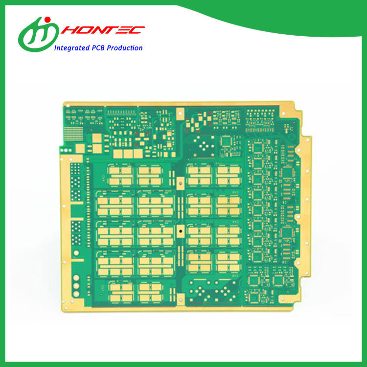
In the world of electronics, the printed circuit board (PCB) is a fundamental component that serves as the backbone of any device. Among the various types of PCBs, the multilayer board stands out due to its ability to accommodate complex circuitry and components in a compact and efficient manner. But how does one manufacture such a sophisticated board? Let's delve into the manufacturing process of a multilayer board.
1. Material Selection
The first step in manufacturing a multilayer board is selecting the appropriate materials. The outer layers are typically made of high-quality materials such as hardwood, like oak or birch, while the inner layers are often composed of softer woods like pine or poplar. These materials are chosen based on their electrical conductivity, mechanical strength, and cost-effectiveness.
2. Cutting and Drilling
Once the materials are selected, they are cut into the desired sizes and shapes using precision cutting machines. Drilling machines are then used to create holes in the layers for component placement and interconnection. These holes, known as vias, are crucial for establishing electrical connections between different layers.
3. Laminating
The next step is laminating, where the individual layers are stacked and bonded together. This is typically done using high-temperature and high-pressure equipment to ensure a strong and durable bond. The lamination process also involves the application of adhesives or prepregs, which are thin sheets of resin-impregnated fiberglass that help bond the layers together.
4. Etching
After lamination, the unwanted copper on the layers needs to be removed to create the desired circuit patterns. This is done through the etching process, which involves applying an etch-resistant mask to the copper layers and then immersing them in an etchant solution. The etchant selectively removes the unprotected copper, leaving behind the desired circuit patterns.
5. Drilling and Plating
Once the circuit patterns are etched, the vias need to be plated with metal to establish electrical connections between the layers. This is done by drilling the vias to the desired depth and then plating them with copper or other conductive materials. The plating process ensures that the vias are electrically conductive and can carry current between the layers.
6. Inspection and Testing
After the plating process, the multilayer board undergoes rigorous inspection and testing to ensure it meets quality standards. This includes checking for defects in the circuit patterns, vias, and plating. Electrical tests are also performed to verify the board's functionality and performance.
In conclusion, the manufacturing process of a multilayer board involves a series of precise and specialized steps. From material selection to final assembly, each step plays a crucial role in ensuring the board's quality, performance, and reliability. The resulting multilayer board is a testament to the precision and skill of the manufacturing process.