
Custom EMC Filter Design Tips for Cleaner Power and Signal Integrity
2026-10-17
Nothing derails a design faster than a filter that looks right on the schematic but lets noise straight through on the board. Custom EMC filter design isn't about exotic parts—it's about matching impedance, layout, and grounding to your actual noise sources. In this guide, we'll share practical tips for building filters that deliver cleaner power and tighter signal integrity. No cookie-cutter solutions. Just the details that help you pass emissions testing without endless trial and error. And if you want a head start, DOREXS specializes in custom filters built around your exact requirements.
Start With the Noise Source, Not the Filter Topology
Many engineers jump straight to picking a filter topology—pi, T, or LC—before measuring what the noise actually looks like. That's backwards. The noise source's impedance and spectral signature determine which filter elements can even work. A low-impedance source feeding a high-impedance load needs a different arrangement than the reverse. Guessing topology first leads to filters that look fine on a schematic but fail on the bench.
Spend time characterizing the source. Use current probes, LISN measurements, or a vector network analyzer to see common-mode versus differential-mode energy, dominant peak frequencies, and how source impedance changes with frequency. Switching converters often produce strong common-mode currents driven by parasitic capacitance, while linear supplies may have low-frequency differential ripple. Without this data, you cannot choose the right insertion loss, component values, or even the correct filter order.
Once the source behavior is clear, the topology almost selects itself. A high-impedance noise source may need a shunt capacitor first; a low-impedance source likely requires a series inductor. Filter design becomes a matter of creating an impedance mismatch at the offending frequencies, not picking a familiar circuit and hoping it fits. Starting from the noise source forces you to solve the real problem instead of reusing a generic topology that only works by accident.
Match Filter Impedance to Your Power Rail's Real Behavior
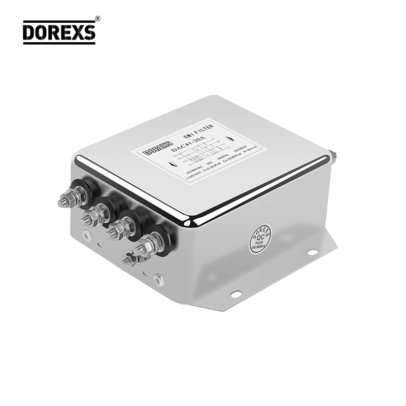
An ideal power rail would present zero impedance across all frequencies, but any real PCB trace, via, or connector adds inductance and resistance that change with switching speeds. When you insert a ferrite bead or LC filter without checking the rail's actual impedance profile, you can easily create a resonant peak that amplifies noise instead of suppressing it. Measure the raw rail impedance from the load's perspective before choosing filter components, because the interaction between the filter and the rail's parasitic elements determines whether you get clean power or a new oscillation.
A common mistake is treating the power rail as a simple DC conductor and selecting filter values from textbook formulas. In practice, the rail's stray inductance and the decoupling capacitors already on the board form a network with multiple resonances. If your filter's output impedance crosses the rail's intrinsic impedance at the wrong frequency, you get a high-Q peak that injects more ripple into sensitive circuits. The better approach is to tune the filter's damping and corner frequency so that the combined impedance stays below the target value across the entire operating band, not just at a single test point.
Pay attention to how the filter behaves under transient loads rather than only steady-state ripple. A rail that looks flat on a network analyzer can still dip or ring when a processor wakes from sleep or an ADC samples. Adding a small series resistor or a lossy ferrite can flatten the impedance curve enough to prevent voltage excursions, but only if you first understand where the rail's real resonances sit. Matching the filter to the measured rail behavior, instead of forcing a generic design, often makes the difference between a quiet rail and one that fights your own components.
Choose Components That Don't Mislead Your Simulation
A model is only as honest as the parts you feed into it. When you grab a component off the shelf, you're not just borrowing its function—you're inheriting every hidden assumption, every smoothing curve, every idealized boundary condition baked into its code. A pump curve that flattens out at high head might look convenient on paper, but if your real system chokes before that point, your simulation is quietly lying to you. The fix starts with asking what each component was originally designed to prove, not just what its datasheet claims.
One practical trick is to place a component in a trivial loop you already know the answer to. If a valve model causes flow to pulse when it should be steady, or a sensor model reports phantom noise at zero input, that's your signal. Another habit worth building: compare component behavior against your own logged data under conditions that stress the edges—low flow, fast transients, near-empty tanks. Often the mismatch only appears when the component is pushed away from the comfortable middle of its operating range, which is exactly where your simulation will end up during a fault scenario.
You also have to watch out for components that are too perfectly clean. Real-world parts drift, stick, and leak a little. If every valve in your model opens in exactly 200 milliseconds with zero hysteresis, the simulation might tell you a sequence is safe when the real one would fault out on a sticky limit switch. Introduce small, documented imperfections yourself—a 5% response delay, a minor leakage path, a deadband on a positioner. These aren't mistakes to hide; they're the details that keep your model from confidently walking off a cliff while you watch the pretty graphs.
Layout Ground Returns Like You're Routing Signals
Ground returns in a PCB layout are often treated as an afterthought, but when routed with the same care as high-speed signals, they quietly transform performance. A well-placed return path reduces loop area, keeping electromagnetic fields tight and noise from wandering into sensitive traces. Think of it as giving the current a predictable road home instead of letting it wander across the board.
Routing returns like signals means paying attention to adjacency. The return current follows the path of least impedance, which usually sits directly under its outgoing trace on a nearby plane. When that plane is cut, split, or interrupted by vias, the current detours, creating larger loops and unwanted coupling. Matching each signal layer with an unbroken reference plane is not just best practice; it is how you stop crosstalk before it starts.
The same discipline applies to differential pairs and clock lines. Their returns need dedicated, continuous pathways that mirror the signal route. When you draw ground returns with the same intent as a critical net, you avoid the slow, intermittent failures that only show up in compliance testing. A board that routes its returns deliberately behaves less like an antenna and more like the controlled system it was designed to be.
Don't Let Parasitic Capacitance Undo Your Common-Mode Choke
A common-mode choke looks straightforward on paper: two windings on a core, canceling differential flux while presenting high impedance to common-mode currents. But at frequencies above a few hundred kilohertz, the winding-to-winding capacitance starts acting like a tiny bypass capacitor across the choke. This parasitic path lets common-mode noise sneak through without being attenuated, so the choke's insertion loss drops off far earlier than the inductance value would suggest.
The parasitic capacitance comes from overlapping turns, adjacent layers, and the physical proximity of the two windings. Every turn next to another forms a small capacitor, and these add up in parallel. In a typical toroidal or split-bobbin design, you might measure tens of picofarads—enough to resonate with the choke's own inductance and create a sharp dip in attenuation right in the frequency range you care about, often between 1 MHz and 30 MHz.
Reducing this effect usually means changing the winding geometry. Splitting the bobbin, adding an insulating barrier between windings, or using a single-layer winding can lower interwinding capacitance. Some designers use a small differential-mode inductor in series to handle the high-frequency residue. Without these steps, the parasitic capacitance quietly erodes the choke's common-mode rejection and leaves your circuit exposed to conducted emissions.
Verify Performance with Real Transient Loads, Not Just Sine Waves
Most bench evaluations still lean on a clean sine wave into a resistive load, which flatters the design and hides the ugly truth. A regulated supply or amplifier that looks stable under steady-state sinusoidal excitation can fall apart when asked to track a fast current step or a ragged load profile drawn from an actual motor, processor, or audio transducer.
Instead of trusting a single frequency sweep, grab the current waveform from a real operating cycle—an inrush event, a burst of PWM-driven switching, or a CPU waking from deep sleep—and feed it to your device under test. Watch the rail for droop, overshoot, and ringing that no sine test will reveal. The difference shows up in phase margin, output impedance, and recovery time, not just THD or ripple.
If you want the design to survive outside the lab, switch your verification load from a signal generator to an arbitrary waveform or an actual application board. Measure how the output recovers from a 0-to-100% load step in microseconds, then compare that to a mild sine perturbation. One test confirms the math; the other confirms the product.
FAQ
Off-the-shelf filters are tuned for generic compliance curves, not your specific switching frequencies or board parasitics. In mixed-signal boards, a one-size-fits-all filter can leave narrowband harmonics right on top of sensitive analog rails, so a custom design lets you place attenuation notches exactly where your converter and clock energy sit.
Start by measuring the unfiltered conducted noise spectrum at the supply input or output, using a current probe or LISN. Identify the dominant peaks and their frequencies. That tells you whether you need differential-mode, common-mode, or both, and whether the problem is broadband switching noise or a specific resonance.
If the required attenuation is less than about 20–30 dB across the band, a single LC stage may be enough. Beyond that, or when you need to cover both low-frequency differential-mode and high-frequency common-mode noise, a multi-stage approach with separate DM and CM chokes plus damping resistors tends to work better without creating a new resonance peak.
Capacitors and inductors stop behaving like ideal C and L above their self-resonant frequencies. A capacitor becomes inductive, an inductor becomes capacitive, and the filter can actually amplify noise instead of attenuating it. So choose parts with self-resonance well above your problematic harmonics, and verify with a network analyzer if possible.
Keep the filter input and output traces separated, minimize the loop area of the high-frequency current path, and place the filter close to the noise source or connector. Use a solid ground pour under the filter components but avoid routing noisy ground return currents through the same via as clean returns. A tiny bit of trace inductance in the wrong place can bypass the filter entirely.
A pure LC filter can resonate at its corner frequency, producing a gain peak that may make noise worse. Adding a small resistor in series with a capacitor across the inductor, or using an RC snubber from the switching node to ground, can damp that resonance while keeping insertion loss high at higher frequencies. The exact value is often best tuned empirically with a signal generator and spectrum analyzer.
Yes, because cleaner power rails reduce jitter in clock buffers and noise coupling into sensitive analog inputs. A well-designed filter also lowers ground bounce and common-mode currents that would otherwise flow through cables and radiate, which directly improves eye margins and ADC/DAC performance on the same board.
Don't test only with a resistive load; real circuits draw dynamic current pulses. Use the actual load or a pulse-load emulator, measure both conducted and radiated emissions before and after, and check the temperature rise of filter components at maximum load. Also, repeat tests with different input cables because their impedance changes common-mode filter behavior.
Conclusion
Designing a custom EMC filter that actually delivers cleaner power and signal integrity starts by ignoring the urge to copy a standard topology. Instead, trace the specific noise source on your board: identify whether it's a switching regulator's ringing, a motor driver's transients, or digital crosstalk. Once you understand where the unwanted energy originates, you can match the filter impedance to the real dynamic behavior of the power rail, not a textbook ideal. A rail that sags under load or resonates at a certain frequency demands a different dampening approach than a stiff, low-impedance bus. Component choice matters just as much; a capacitor that looks perfect in a simulation can mislead you if its parasitic inductance and DC bias derating are ignored. Select parts with measured high-frequency characteristics and place them so their physical pads don't add hidden loops.
Layout is where many custom filters quietly fail. Route the filter's ground return as carefully as a high-speed signal, keeping noisy return currents away from clean analog grounds and using short, wide traces to cut loop area. A common-mode choke only works when parasitic winding capacitance doesn't create an unintended bypass path, so wind or select chokes with controlled interwinding capacitance and keep adjacent planes from coupling. Finally, verify the filter under real transient loads, not just steady sine waves—switch the actual load on and off, inject load steps, and probe rail ripple and signal integrity simultaneously. This exposes resonances and saturation effects that a swept sine test misses. By treating the filter as a noise-source-specific, layout-sensitive, transient-tested system, you get cleaner power without sacrificing signal margins.
Contact Us
Contact Person: Eric
Email: [email protected]
Tel/WhatsApp: 8618117837140
Website: https://www.emcdorexs.com